Introduction: The Nanoscale Revolution Waiting to Happen
For over a decade, two-dimensional (2D) materials like graphene and molybdenum disulfide (MoS₂) have been the superstars of materials science. Thinner than a single strand of human DNA, these atomic-scale sheets possess extraordinary electronic properties that promise to revolutionize computing — from ultra-fast transistors to hyper-efficient memory. They represent a potential path to continue the incredible progress of Moore’s Law, pushing beyond the physical limits of silicon.
But there’s a catch. For all their brilliance in the pristine, controlled environment of a research lab, moving these materials into the complex, messy world of commercial chip manufacturing has been a monumental challenge. It’s one thing to create a single, perfect 2D transistor; it’s another thing entirely to integrate thousands or millions of them onto a standard silicon chip and have them all work together reliably. This is the infamous lab-to-fab gap — a chasm that has kept many groundbreaking technologies from reaching the real world.
A recent paper published in Nature tackles this problem head-on. Researchers have developed a comprehensive blueprint called ATOM2CHIP — a complete strategy for bridging the gap between a single atomic device concept and a fully functional, packaged chip. Using this blueprint, they successfully built a 1-kilobit 2D NOR flash memory chip, demonstrating a viable pathway for integrating the advantages of 2D electronics into practical, system-level applications. This work isn’t just another incremental improvement; it’s a detailed roadmap for the future of electronics.
The Great Integration Challenge: When Two Worlds Collide
To appreciate the scale of this achievement, we first need to understand why integrating 2D materials with traditional silicon CMOS (Complementary Metal-Oxide-Semiconductor) technology is so difficult. It’s a story of mismatch at almost every level.
1. The Physical Mismatch:
A standard CMOS wafer, even after being polished, presents a rugged landscape at the atomic scale. Its surface has a roughness of 1–2 nanometers due to the dense, underlying circuitry. Now, imagine trying to lay a perfect, single-atom-thick sheet of MoS₂ (less than 1 nm thick) over this bumpy terrain. The 2D material gets stretched, wrinkled, and stressed — leading to unpredictable electrical behavior and a high rate of device failure.
2. The Electrical Mismatch:
2D devices often operate on different rules than silicon. For instance, the 2D flash memory in this study requires negative voltages for certain operations. Applying negative voltage to a standard CMOS circuit can trigger parasitic PN junctions, causing massive current leakage and potentially frying the chip — a phenomenon known as latch-up.
3. The Packaging Problem:
Chip packaging — the process of enclosing the silicon die in a protective casing with pins to connect to the outside world — is a brutal affair. It involves high temperatures, mechanical pressure, and the risk of electrostatic discharge (ESD). For robust silicon, this is routine. For a fragile, atomically thin material, it can be a death sentence.
Solving these issues requires more than just a better 2D transistor. It demands a holistic approach that rethinks the entire fabrication and design process from the ground up. This is precisely what the ATOM2CHIP blueprint provides.
The ATOM2CHIP Blueprint: A Two-Pillar Strategy
The researchers’ ATOM2CHIP technology is a masterclass in system integration, built on two core pillars:
- A Full-Stack On-Chip Process to solve the physical fabrication challenges.
- A Cross-Platform System Design to solve the electrical and logical compatibility issues.

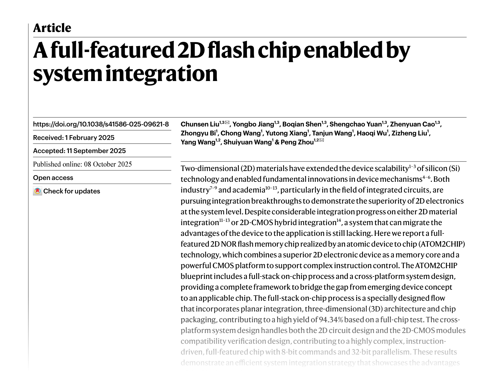
Figure 1: The ATOM2CHIP blueprint outlines the full-stack process and system design. The researchers fabricated CMOS dies on an 8-inch wafer and integrated a 2D flash module on top, creating a hybrid chip with a clear 3D structure.
Pillar 1: The Full-Stack On-Chip Process (The “Hardware” Solution)
This pillar focuses on building a reliable 2D memory array directly on top of a finished CMOS wafer. The authors developed a three-part strategy to achieve an impressive final yield of 94.34%.
Step 1: Conformal Adhesion on a Rough Surface
To solve the surface roughness problem, the researchers developed a conformal adhesion process. Instead of simply placing the 2D material on the chip, they used a special gradual-release transfer technique followed by multiple annealing (heating) steps. This allows the atomically thin MoS₂ layer to gently conform to the bumpy CMOS surface — much like cling film — relieving mechanical stress that would otherwise degrade device performance.

Figure 2: The full-stack process addresses key hardware challenges. The modular 3D architecture separates the 2D and CMOS components. Despite the CMOS die’s rough surface, the conformal adhesion process ensures high-quality 2D device integration, leading to uniform performance. Specialized packaging protects the fragile 2D materials.
As shown in Figure 2d, devices built with this process have tight, well-separated “ON” and “OFF” state threshold voltage distributions — a hallmark of high uniformity and reliability. Without this process, the distributions would be wide and overlapping, rendering the memory unreliable.
Step 2: A Modular 3D Architecture
Rather than forcing direct cell-to-cell compatibility between 2D memory cells and silicon logic, the team adopted a modular approach. They treated the 2D NOR flash array as one functional module and the CMOS platform as another, fabricating them separately and connecting them vertically via Through-Glass Vias (TGVs). This converts a thorny device-level incompatibility problem into a manageable interface design challenge.
Step 3: 2D-Friendly Packaging
To protect the delicate 2D material during packaging, the researchers implemented a multi-layered protection strategy (Figure 2e):
- Region-Specific ESD Protection: Custom ESD circuits were placed on all pads to prevent static damage to the 2D layers.
- Low-Impact Bonding: They employed room-temperature ultrasonic bonding instead of high-temperature thermocompression, reducing post-packaging leakage by more than tenfold.
- Gentle Adhesives: A room-temperature curing adhesive minimized thermal damage during die attachment.
Thanks to these measures, the resulting 2D flash cells are high-yield and high-performance — with exceptionally fast 20-nanosecond program/erase speeds and ultra-low energy consumption of 0.644 picojoules per bit.
Pillar 2: Cross-Platform System Design (The “Circuit & Software” Solution)
Building the hardware is only half the battle. The next challenge is making the 2D and CMOS modules operate seamlessly together. This demanded a co-design methodology where the behavioral characteristics of the 2D device informed the CMOS circuit design.

Figure 3: Cross-platform compatibility verification ensures CMOS modules are tailored to the 2D memory. Isolated transistors tolerate local negative voltages, optimized buffer chains provide fast driving, and improved sense amplifiers deliver reliable reading. The entire system, such as a 32-bit parallel programming operation, is validated through simulation.
Step 1: Designing a Crosstalk-Free 2D Memory Circuit
The researchers opted for a NOR flash architecture for high speed. A major issue in memory arrays is crosstalk, where operating on one cell affects neighbors unintentionally. They implemented a half-selected scheme: while the selected cell receives full programming voltage \(V_{\text{pp}}\), adjacent cells see only half that voltage (\(\frac{1}{2}V_{\text{pp}}\)). Since Fowler–Nordheim tunneling is exponentially sensitive to voltage, this halving effectively suppresses unwanted programming.

Figure 4: Crosstalk suppression using the half-selected scheme. The selected cell (red) receives full voltage, while neighboring cells (blue) see half, preventing accidental programming due to the exponential voltage dependence of tunneling.
Step 2: Making CMOS Tolerate Negative Voltage
To accommodate the negative voltage requirements of the 2D flash cells, specialized silicon transistors were designed for the interface circuits (Figure 3b). An isolation ring and a deep N-well create a locally isolated pocket within the substrate, enabling negative biasing without affecting the rest of the chip — avoiding latch-up and leakage.
Step 3: Impedance Matching for Driving and Sensing
Reliable writing and reading require precise impedance matching:
- Driving Ability: The buffer circuits driving word lines and bit lines were designed using the logical effort method to create a multi-stage inverter chain (Figure 3c). This amplifies small logic signals into fast, clean pulses capable of driving the memory lines efficiently.
- Sensing Ability: Reading cell states demands sensing tiny currents (~100 nA). Initial sense amplifier design (SA1) failed due to slow bit-line voltage discharge from large parasitic capacitance.

Figure 5: SA1 struggled with bit-line capacitance (CBL), leading to slow VBL discharge and misreads within the timing window.
The improved 2D-compatible design (SA2) added a switch transistor that isolates the sense amplifier from bit-line capacitance during sensing, cutting read time by 70% and ensuring accuracy.

Figure 6: SA2’s design isolates the sense amplifier from the large bit-line capacitance, allowing quick voltage settling and accurate readout.
With these elements integrated, simulations confirmed that the complete chip could handle advanced, instruction-driven operations: 32-bit parallel programming, full-chip erasing, and random-access reads.
The Moment of Truth: Full-Chip Testing
The final packaged 2D NOR flash chip was tested using a system built around an FPGA, with commands issued from a host computer to evaluate real-world operation.

Figure 7: Full-chip functional demonstration. The test system and internal data flow were used to validate performance. A checkerboard programming test showed 93.55% accuracy across all 32 word lines, confirming reliability and effective crosstalk suppression.
Key results:
- High Yield: Operational yield of 94.34% — on par with mature silicon.
- Full Functionality: Running at 5 MHz, the chip executed 8-bit commands for 32-bit parallel program, read, and erase operations.
- Checkerboard Programming Test: Achieved 93.55% accuracy, with only a handful of errors — validating system robustness.
While peripheral CMOS power consumption was comparable to commercial NOR flash, the ultra-low energy to program the 2D cells offers clear advantages for applications like IoT and embedded devices.
Conclusion: A Blueprint for the Future
This research marks a significant milestone in 2D electronics. The ATOM2CHIP blueprint is more than a singular success — it’s a complete methodology addressing physical, electrical, and architectural barriers to merging nanomaterials with mainstream silicon. By strategically tackling challenges across materials science, fabrication processes, circuit design, and system architecture, the researchers have laid a credible path from lab to fab.
This 1-Kb chip is a first step, but an important one: it demonstrates that the nanoscale revolution can now progress beyond isolated device prototypes, enabling complex systems that harness the unique strengths of 2D materials. The future of electronics just moved one step closer.